Autonomous Wireless Sensor Node
A solar-powered sensor node that regulates its own charging, measures temperature, and transmits over Bluetooth without a wired supply
Overview
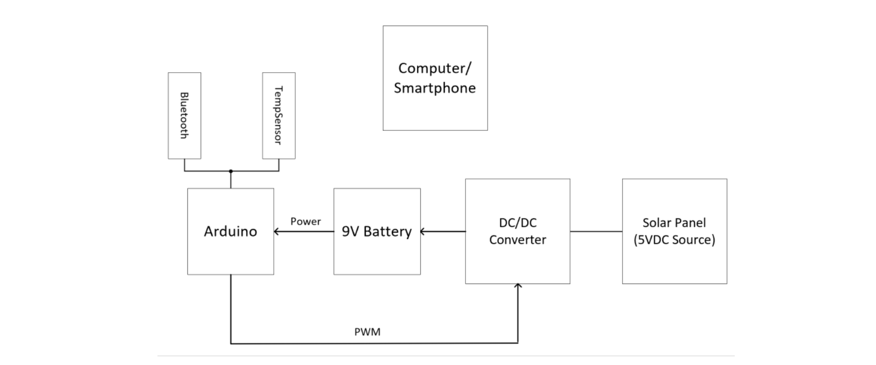
The wireless sensor node integrates a DC/DC boost converter, a 9 V rechargeable battery, an ATmega328P microcontroller, and a thermistor-based temperature sensor. A 4–5 V power supply was used to simulate solar input during development and testing.
The microcontroller regulates the converter's output voltage, processes temperature readings, and transmits system data over Bluetooth. When the input source is unavailable, the node switches to battery power and enters a low-power operating mode.
System Architecture
The system is organized into three interconnected functions: power management, sensing and control, and wireless communication.
POWER MANAGEMENT
SENSING & CONTROL
The microcontroller also receives converter-voltage feedback and generates PWM to regulate the power stage.
Boost Converter Design
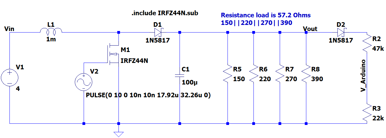
The boost converter was designed to step up a 4–5 V input to approximately 9 V while meeting a switching-frequency requirement of at least 30 kHz and an output-ripple target below 90 mV.
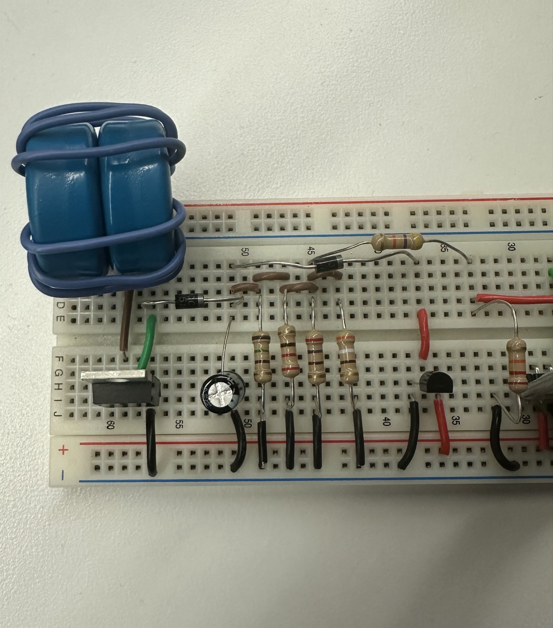
The circuit uses an IRFZ44N MOSFET, a 100 µF output capacitor, and a hand-wound 1 mH inductor constructed with 11 turns on a double magnetic core. Component values were determined from the converter's voltage, current, and ripple requirements before the circuit was modeled in LTspice.
LTSPICE
8.68 V
Simulated output
10.60 mV ripple amplitude
HARDWARE
8.35 V
Measured output
5.55 mV ripple amplitude
The initial open-loop measurements confirmed that the physical converter operated below the ripple limit, although its output voltage was lower than the nominal target. Oscilloscope measurements of the MOSFET drain-source voltage and inductor current were also used to examine switching behavior. A 1 Ω shunt allowed inductor current to be calculated from the measured voltage waveform.
These measurements provided the basis for verifying the hardware before enabling microcontroller-based voltage regulation.
Closed-Loop Regulation & Battery Charging
The ATmega328P generates PWM using Timer2 in Fast PWM mode at approximately 31.372 kHz. A resistor divider scales the converter output into the microcontroller's ADC range, allowing the firmware to adjust the MOSFET duty cycle in response to changes in output voltage.
To verify the feedback system, the input voltage was varied across three operating points while monitoring the converter output.
Experimental results from the closed-loop regulation test. The output varied by only 0.13 V across the 4–5 V input sweep.
The feedback controller maintained the boosted output between 9.63 V and 9.76 V across the tested input range. A separate battery-charging test recorded the battery voltage increasing from 8.8 V to 9.0 V, confirming that the regulated converter could supply charging power.
Converter Efficiency
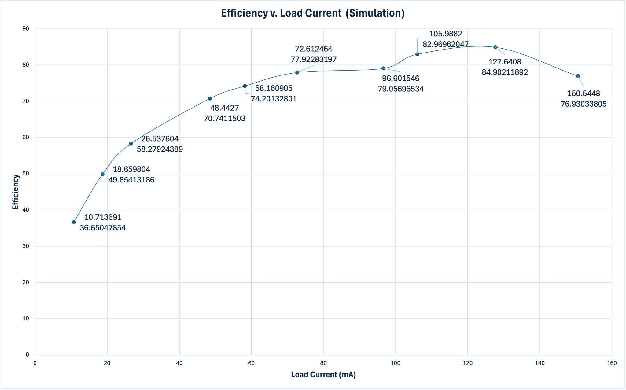
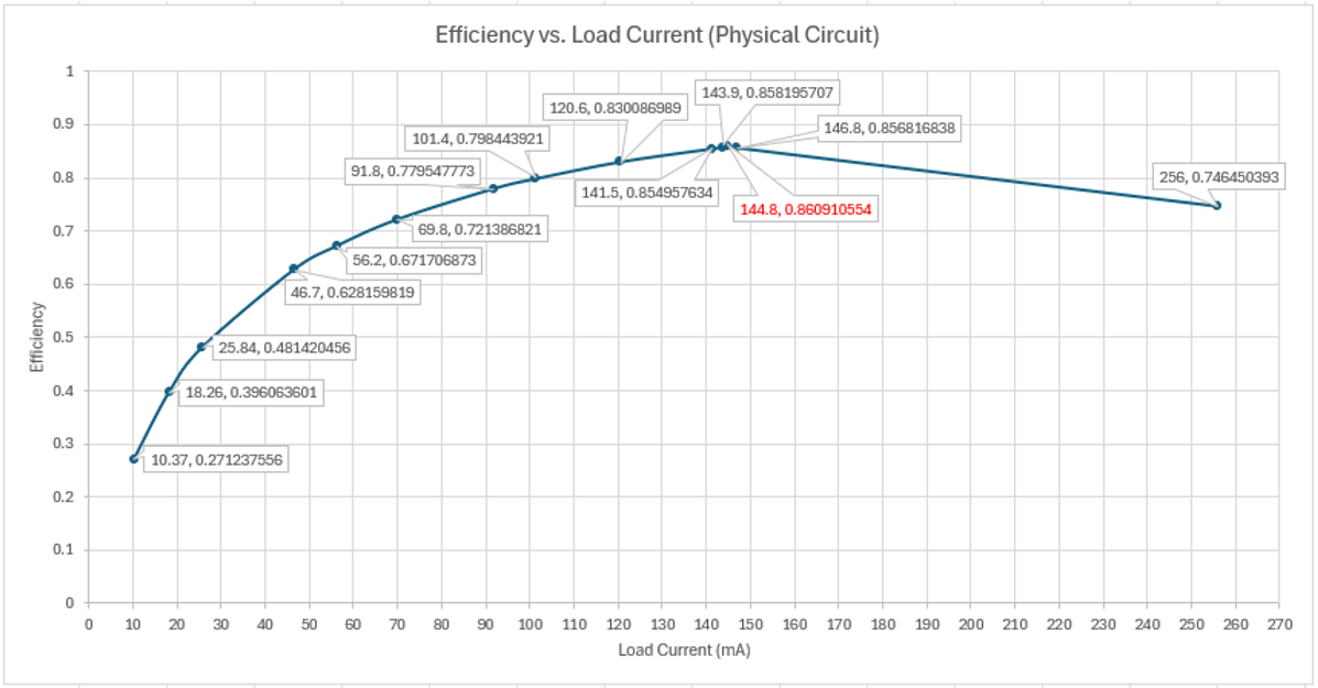
Converter efficiency was characterized across resistive loads by measuring input and output voltage and current, then calculating the ratio of output power to input power.
PEAK MEASURED
86.1%
At 144.8 mA output load current
PEAK SIMULATED
84.9%
The hardware efficiency curve peaked near a 145 mA load and decreased at lighter loads. Characterizing the converter across its operating range helped identify where the physical circuit transferred power most efficiently rather than relying on a single nominal operating point.
Temperature Sensing & Bluetooth Communication
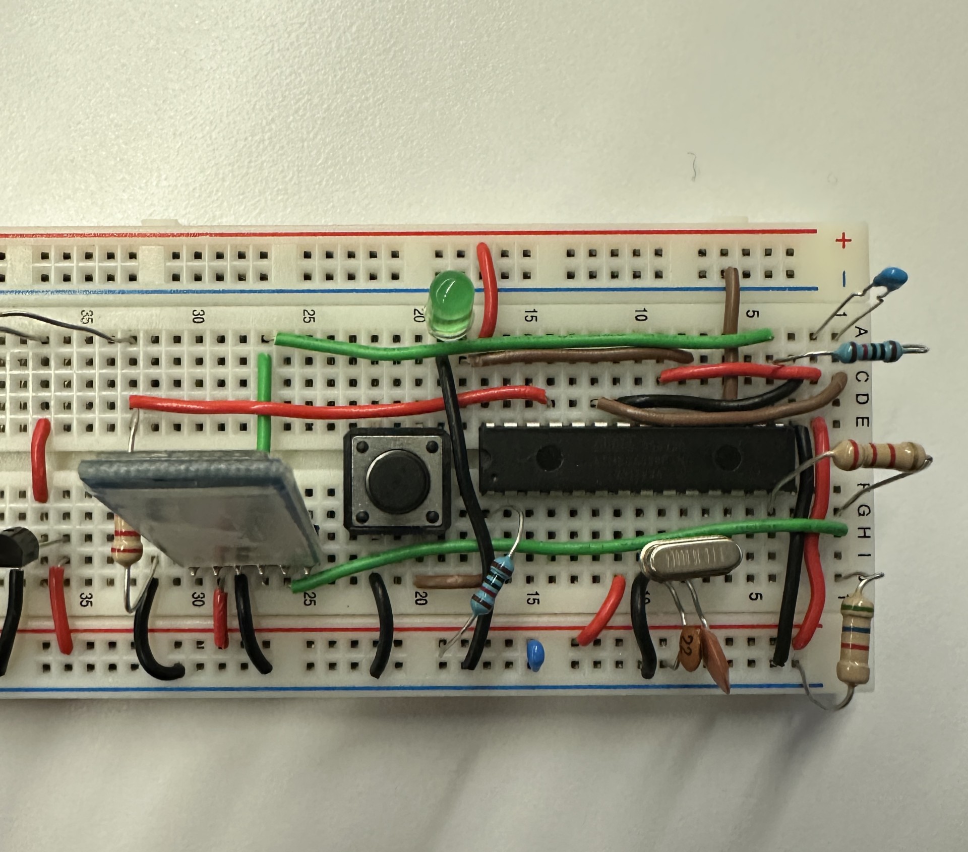
Temperature is measured using a 10 kΩ thermistor and a 10 kΩ reference resistor configured as a voltage divider. The ATmega328P samples the divider through its ADC, calculates thermistor resistance, and applies the Steinhart–Hart equation to convert the reading into temperature.
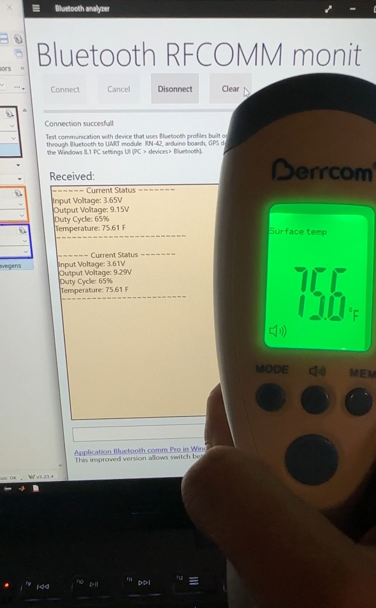
The microcontroller transmits temperature and system telemetry through its UART-connected Bluetooth module. A resistor divider reduces the microcontroller's 5 V transmit signal to approximately 3.3 V for the Bluetooth interface. The receiving application displays temperature, input and output voltage, and converter duty cycle.
The temperature measurements were checked against a commercial infrared thermometer at approximately 64 °F, 75.6 °F, and 80.2 °F. The recorded comparisons showed differences of up to 0.6 °F, providing experimental validation of the sensing and wireless transmission system.
Low-Power Operation
When the input source is disconnected, the microcontroller stops regulating the converter and transitions to battery-powered operation. The firmware disables the ADC and brown-out detection before entering power-down sleep, using the watchdog timer to wake the microcontroller periodically for sensing and communication.
For the battery-only endurance test, the system was configured to transmit data at 11-minute intervals. Current consumption was measured across a 1 Ω shunt resistor to compare active and power-saving operation.
ACTIVE MODE
18 mA
POWER-SAVING MODE
15 mA ↓ 16.7%
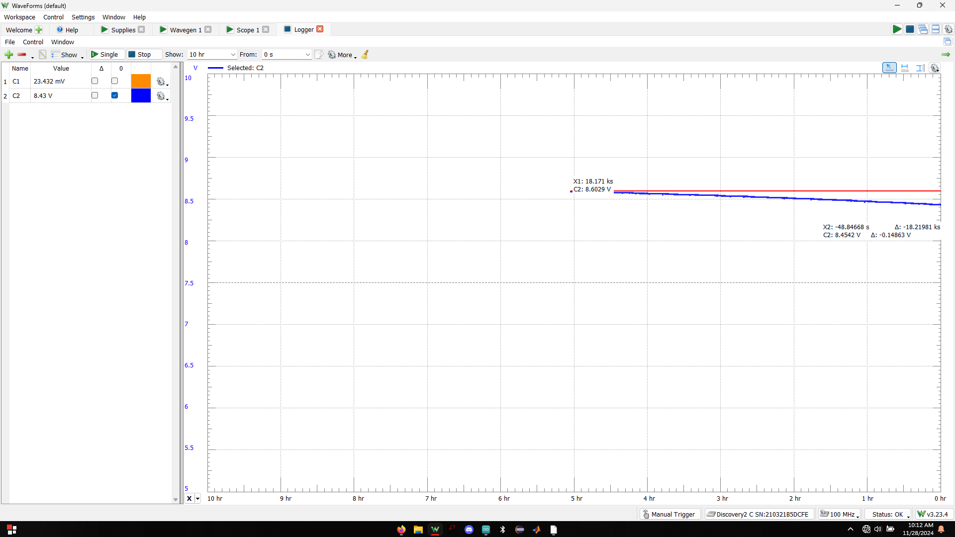
During a five-hour battery-only test, battery voltage decreased from 8.6092 V to 8.4542 V. The measurements confirmed continued operation without an external power source while documenting the discharge behavior of the prototype.
That 0.155 V drop over five hours corresponds to a decay rate of 31 mV per hour. Extrapolating the rate across the battery's usable range estimates how long the node can run without an input source.
OPERATING RANGE (9–7 V)
64.52 h
≈ 2.7 days
THEORETICAL MAXIMUM (9–0 V)
290.32 h
≈ 12.1 days